
-
Contact Us Today!
If you have any questions about packaging technology or would like to discuss your requirements regardless of where you are in the design cycle or procurement phase, please click on the link above.
-
Follow us on LinkedIn!

About
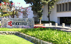
Kyocera offers a broad line of semiconductor package products and services based on advanced ceramic and plastic material technologies. In North America, these products and services are provided by the Semiconductor Components Group of Kyocera International, Inc. of San Diego, California.
By expanding to manufacture semiconductor packages here in 1971, Kyocera became the first Japanese-owned company with production operations in the State of California. From there, our San Diego team has continuously built upon Kyocera's legacy of designing and mass-producing package solutions for the industry's most demanding requirements.
In 1987, we began operating a maquiladora in Tijuana, Mexico known as Kyocera Mexicana, S.A. de C.V. (KMX). Since then, our expanding capabilities both in San Diego and Tijuana have allowed us to increase throughput and shorten cycle times for our customers. At the same time, the continued growth of Kyocera's North American Operations has created new divisions and entirely new companies in a wide range of markets.
Over the past three decades, Kyocera's Semiconductor Components division has grown tremendously both in North America and abroad by supporting the development of wireless telecommunications, personal computing, the Internet, automotive electronics and intelligent medical devices. We will continue to grow by meeting and exceeding our customers' expectations over the next three decades and beyond.