
-
Contact Us Today!
If you have any questions about packaging technology or would like to discuss your requirements regardless of where you are in the design cycle or procurement phase, please click on the link above.
-
Follow us on LinkedIn!

Contract Assembly
Kyocera first opened its Assembly Technologies Division in 1995 to meet the demand for package assembly. Since then, the division expanded to include two Flip Chip assembly lines due to the exponential market growth in digital and high frequency applications. Multichip module assembly followed as the demand for Hi-Rel outsourced assembly increased, enabling our customers to focus on their core competencies and reduce operational costs.
Advances in semiconductors and passive components are the drivers for high-performance packaging and assembly that can be optimized and tailored for specific applications. Kyocera International's contract assembly offers design and engineering support, BOM procurement, and a wide selection of substrate and circuit board materials.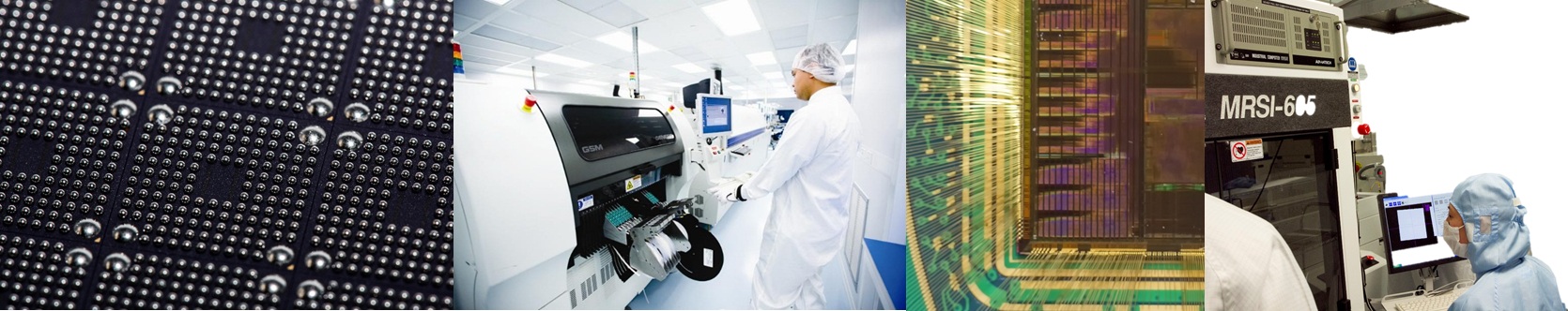
Markets and Applications
- Commercial / Government / National Laboratories
- Hi-Rel Aerospace & Communication
- CCD/CMOS Image Sensor
- High-End Server / Test Equipment
- Night Vision
- Atomic Clock
- Downhole-Drilling
- Biotech / Medical
- Others
Assembly Technologies
- Fine Pitch Wire Bond and Flip Chip Assembly
- MCM / Complex Module Assembly
- RF / MW
- Power Electronics Package Assembly
- MEMS with proprietary getter options
- Hermetic and Non-Hermetic Sealing
- Vacuum Solder
- Polymer Core BGA
- Wafer Scribing / Marking
- New Product / Process Development
- Advanced Ceramic Substrates / Modules
- Organic Substrates / PCB
- Small to Large Volume
- Quick-turn