
Kyocera Expands U.S.-Based Semiconductor Assembly Capabilities, Capacity, and Technology Investment
Company’s “one-stop solution” offers comprehensive onshore semiconductor packaging and OSAT services from 288,000sf facility in California
- Corporate
- Semiconductor Components & Assembly Services
SAN DIEGO, CALIF. – Oct. 3, 2023 – Kyocera International, Inc. today announced an expansion of its U.S. semiconductor and microelectronic device assembly capabilities at its manufacturing operations in San Diego, Calif., where the company has produced high-performance semiconductor packaging products for more than 50 years.
In response to U.S. semiconductor industry demand for domestic complex assembly capabilities that support rapidly advancing technologies, Kyocera’s latest investments in San Diego have recently:
- Doubled assembly cleanroom space
- Tripled surface-mount component-attach capacity
- Added wafer laser-grooving and wafer-bumping capabilities
- Introduced all-new 0.3µm-placement-accuracy bonding equipment
Together, Kyocera’s new capabilities in U.S.-based “OSAT” — Outsourced Semiconductor Assembly and Testing — will enable further adoption of 2.5D and 3D packaging methodologies.
“The U.S. semiconductor industry needs deeper on-shore engineering support during the design, process development, and production of IP-sensitive products,” said Franklin Kim, Vice President of Kyocera’s Semiconductor Components Group in San Diego. “Kyocera can provide this support with state-of-the-art semiconductor package manufacturing and materials to help ensure complex devices are designed for manufacturability at the highest yields — using ceramic, high-density build-up (HDBU) organic, printed wiring board (PWB) organic, or alternative material substrates.”
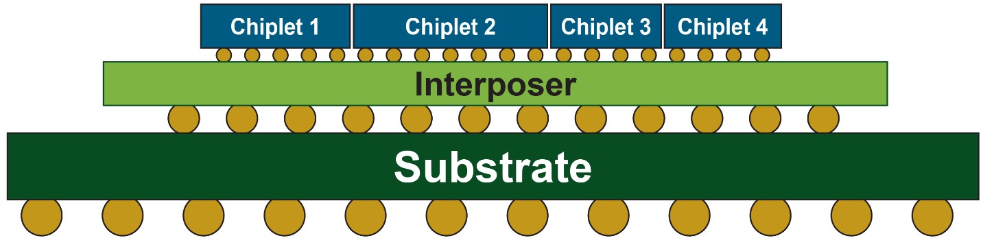
Illustration: Cross-sectional view showing chiplets in 2.5D integrated circuit (2.5D IC) packaging, an advanced technology that combines multiple semiconductor chips into a single package.
Kyocera’s capabilities in San Diego include both 2.5D and 3.0D semiconductor device assembly and testing.
San Diego-based Kyocera International, Inc., a subsidiary of Kyocera Corporation, has been advancing the technology of semiconductor package manufacturing in the U.S. since Silicon Valley’s emergence as a tech cluster in 1971.
Kyocera Corporation (TOKYO:6971, https://global.kyocera.com/), the parent and global headquarters of the Kyocera Group, was founded in 1959 as a producer of Fine Ceramics (also known as “advanced ceramics”). By combining these engineered materials with metals and integrating them with other technologies, Kyocera has become a leading supplier of industrial and automotive components, semiconductor packages, electronic devices, smart energy systems, printers, copiers, and mobile phones. During the year ended March 31, 2023, the company's consolidated sales revenue totaled 2.0 trillion yen (approx. US$15.1 billion). Kyocera is ranked #671 on Forbes magazine’s 2023 “Global 2000” list of the world’s largest publicly traded companies, and has been named by The Wall Street Journal among “The World's 100 Most Sustainably Managed Companies.”