


Total Semiconductor Packaging Solutions Provider
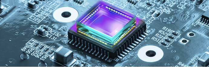
Kyocera is a leading provider of advanced ceramic and organic semiconductor packaging and assembly services, offering custom-engineered and standard solutions. Kyocera empowers customers to achieve superior performance and accelerate success by combining innovative designs with highly optimized processes.
Advanced Ceramic and Organic Semiconductor Package Solutions and Assembly Services
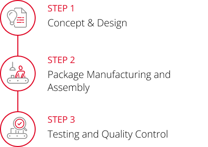
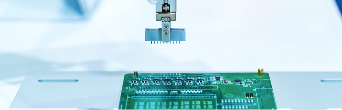
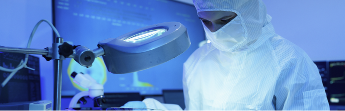
Kyocera established its North American operations in California in 1971 and has become a leading provider of advanced ceramic packaging solutions and highly reliable assembly services for challenging applications. Kyocera’s San Diego facility leverages vertically integrated, tightly controlled manufacturing processes to deliver exceptional performance and reliability for mission-critical applications. With its comprehensive, end-to-end production capabilities, the facility is optimized for scalable, high-mix production, efficiently delivering volumes ranging from single-unit builds to large-scale programs while maintaining strict quality and process controls.
-
100% U.S.-Based and
U.S. Government RegisteredWith certifications in:
- ISO 9001:2015 (pdf/605.3 KB)
- ISO 14001:2015 (pdf/606 KB)
- ISO 13485:2016 (pdf/710.7 KB)
- ISO 45001:2018 (pdf/455.7 KB)
Capabilities

Applications


About Us

With over 50 years of manufacturing expertise, Kyocera delivers semiconductor packaging solutions engineered for optimal integrity and superior performance. Kyocera’s extensive knowledge of materials and processes enables it to meet the rigorous demands of advanced packaging requirements.
Kyocera is committed to innovation and operational excellence at every stage of development, from substrate and package design to highly optimized, precision-controlled assembly processes, ensuring consistent performance, reliability and quality.
View All