
Capabilities
Assembly Process Capabilities
Kyocera provides comprehensive U.S. based semiconductor assembly services with a factory in San Diego, California; technical resources in Boston, MA; Dallas, TX; and Milpitas, CA. We are a top contract manufacturer with experienced engineering staff, world-leading facilities, and state-of-the-art equipment, offering custom services tailored to each customer’s requirements. Our design support ensures that manufacturability is built-in from the start, with state-of-the-art simulation capabilities and process control expertise. From single-piece prototypes to full turnkey solutions, supporting annual volumes in excess of 250,000 pieces, Kyocera’s Assembly team is here to serve you.
Our Capabilities
Design
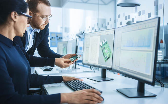
Kyocera encourages customers to engage with us at the design stage. Our guidance on material selection and process development can optimize your design for manufacturability.
Using the combined resources of our assembly and substrate design teams, Kyocera can offer a total product review to provide our customers that ultimate solution.
Inventory Control
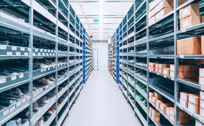
Kyocera’s Assembly Technologies Division can support fully consigned assembly or a complete turnkey model, with material traceability either way. For turnkey orders, we can provide accurate pre- and post-assembly materials assessments and maintain inventory.
Wafer Processing
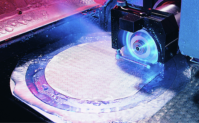
Kyocera offers wafer-level assembly services as a standalone solution or as part of a complete assembly operation. We currently offer the following wafer operations:
- Wafer Bumping (up to 300mm)
- Laser Grooving
- Back Grinding
- Wafer Dicing
- Die pick
- Die Traceability
Substrates
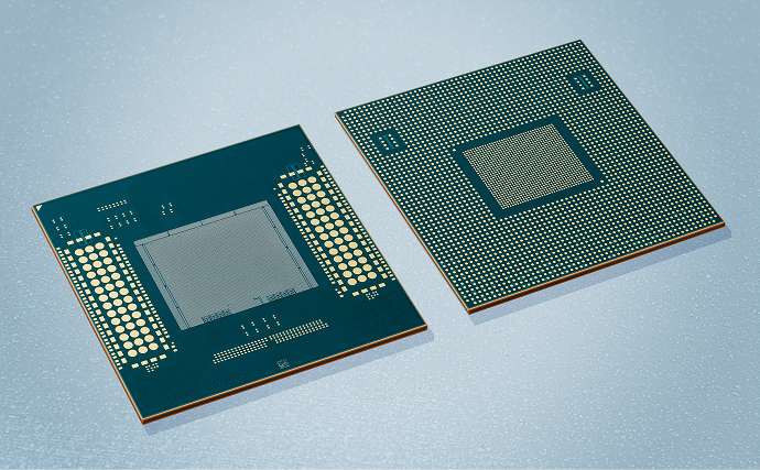
Kyocera provides both ceramic and organic packages for Large Scale Integration (LSI) devices. In addition to alumina (Al2O3) ceramics, we produce aluminum nitride (AlN) with high thermal conductivity (150W/mK), as well as Low Temperature Co-Fired Ceramic (LTCC) packages with high (12.3ppm/K) and low (3.4ppm/K) coefficients of thermal expansion.
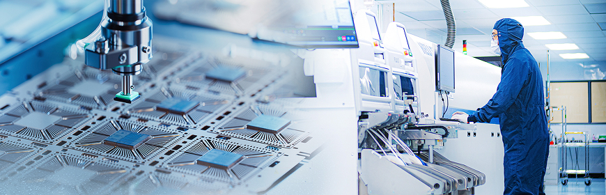
Assembly
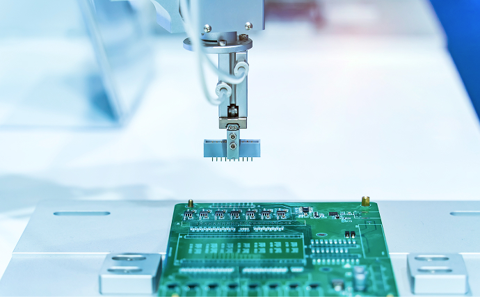
Kyocera has more than 35,000sf of cleanroom assembly space in San Diego, and approx. 7,000sf in Tijuana, Mexico. Together, these facilities can provide redundant lines for business continuity, and location options to support various business models. These facilities continually add capacity and state-of-the-art capabilities for sophisticated mixed-technology devices, including Multi-Chip Modules (MCMs) and 2.5D + 3D assemblies that may require:
- Wafer processing
- Circuit Card Assembly (CCA)
- Surface Mount Technology
- Flip Chip Assembly
- Wire Bond Assembly
- Fine Pitch Bonding (reflow / thermo-compression / thermo-sonic)
- Lid Fabrication + Getter and Absorber attachment
- Sealing/Lidding
- Marking
- Pre-tin
- Environmental Testing
- Electrical Testing
- Ball Grid Array services
Failure Analysis
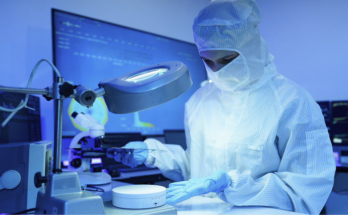
Kyocera conducts failure analysis in-house for faster turnaround in identifying root causes. Our strong relationships with third-party labs cover any analysis we cannot complete internally, and the following services can all be performed on-site:
- SEM w/ EDS capabilities
- Mounting and cross-section
- PLAP
- X-ray scans
- CT scans
- Sonoscans
- Pull & Shear
- Hermetic leak testing
- Non-contact metrology
- Laser profilometer
- Differential Scanning Calorimetry (DSC)
Advanced Assembly Technology Processes
Discover our advanced assembly technology processes, where precision engineering meets innovation. From material preparation to final inspection, our solutions optimize microelectronic and board-level assembly to the highest performance levels for all markets and applications, including AI, 5G, medical devices, and others.