
Applications
Semiconductor Package Applications
Kyocera offers a wide selection of semiconductor package solutions in the areas of Data & Telecom, AI & Data Centers, Medical & Biotech, MEMS & Sensors, Photonics, and Space & Satellite applications.The combination of Kyocera's advanced material technologies, manufacturing processes, and design capabilities allows us to provide high-quality packaging and service solutions to meet customer needs in the most demanding applications.
Our Applications
Data & Telecom

Microelectronic technology is crucial in data and telecom networks, enabling faster data transfer and clear voice communication. Our robust packaging maximizes device and system performance for fast-growing AI applications. Additionally, within the RF chain for power amplification in network base stations (operating from 500 MHz to 1.9 GHz and beyond), Kyocera products include surface mountable ceramic and, AlN packages for, power electronics, and mixed-signal devices. Further, Kyocera is also a leading supplier of power transistor packages, for LDMOS, GaN, SiC, and related devices, driving the advancement of telecommunications technology.
AI & Data Center

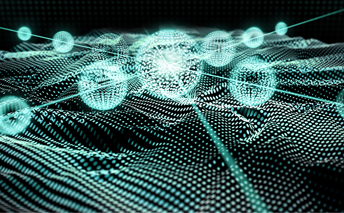
Artificial Intelligence and hyperscale data centers require unprecedented system performance, bandwidth, and energy efficiency. Advanced semiconductor packaging is a critical enabler of these trends. Kyocera’s comprehensive assembly and packaging solutions are designed to support high-performance computing (HPC), AI accelerators, and next- generation data center architectures.
Medical & Biotech

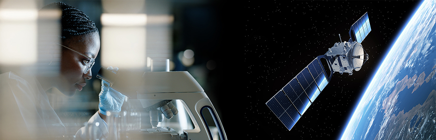
Kyocera’s materials and technologies are vital to medical electronics, providing reliable microcircuitry for devices ranging from DNA sequencers to CAT scanners. Our packages and substrates facilitate innovations in healthcare technology, including wireless multimedia transmission, secure data transactions, and telemetry for the growing IoT market. Kyocera’s solutions include ceramic packages that provide unique performance advantages, including chemical inertness, thermomechanical stability, and hermeticity. We offer various package types such as BGA, MEMS, microfluidic, mixed signal, image sensor, flip chip, and feedthroughs, to meet the most challenging demands.
MEMS & Sensors
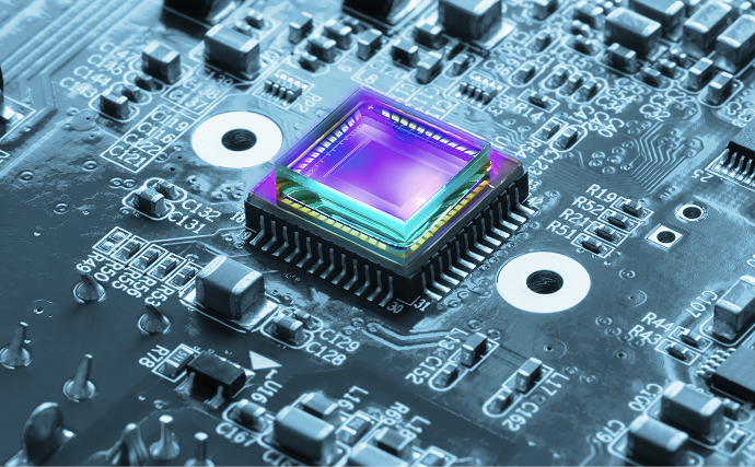
Kyocera optimizes the excellent hermetic capabilities of ceramic materials for packaging sensitive MEMS chips and image sensors. Our MEMS and Sensor packages offer cost-effective solutions for a wide variety of applications, such as cameras, automotive systems, RF equipment, video displays, scanners, medical diagnostics and other high-reliability electronics. LCC, BGA, and SMT packages are often used for these devices. We offer assembly for MEMS and Sensor devices in our Class 1,000 and Class 100 clean rooms in San Diego.
- LCC
- Cavity-style BGA or PGA
Photonics
Electronics and optics converge in the photonics sector to create sophisticated new devices and technologies. Photonic devices provide precise control over light sources, modulation, and signal processing, significantly improving the performance and efficiency of lasers, photodetectors, and optical communication systems. These minute components will be essential to new breakthroughs in high-speed data networks, AI, laser-based manufacturing, and medical imaging. At Kyocera, we are dedicated to delivering state-of-the-art microelectronic solutions that drive innovation and growth within the photonics industry.
Space & Satellite
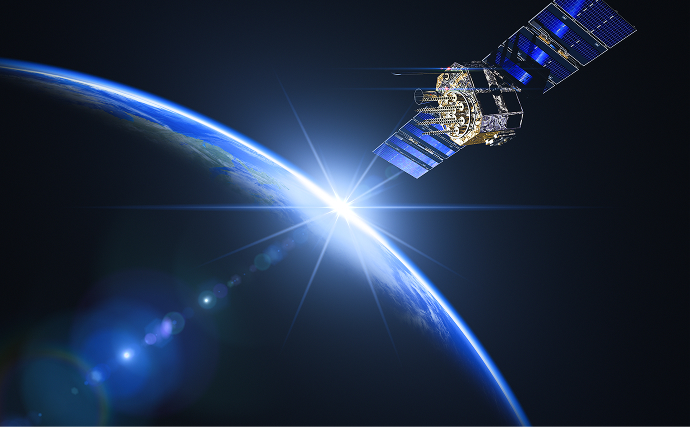
Space and Satellite applications demand enhanced performance, often in harsh environments, with life cycles that exceed requirements for commercial electronics. Kyocera is a critical supplier of advanced, dual-use ceramic packages for radar systems, on-board communication, night vision devices, and satellites, with a long history of providing MIL-STD-883 tested hermetic packaging.
Packages and Modules for Space & Satellite Use
- Transmit / Receive Modules
- High-Frequency MMIC Hermetic Package
- ASICs
- MCMs
- Multilayer BGAs